- 您现在的位置:买卖IC网 > Sheet目录3882 > PIC16F87T-I/ML (Microchip Technology)IC MCU FLASH 4KX14 EEPROM 28QFN
121
8008H–AVR–04/11
ATtiny48/88
The PRSPI bit in “PRR – Power Reduction Register” on page 40 must be written to zero to
enable the SPI module.
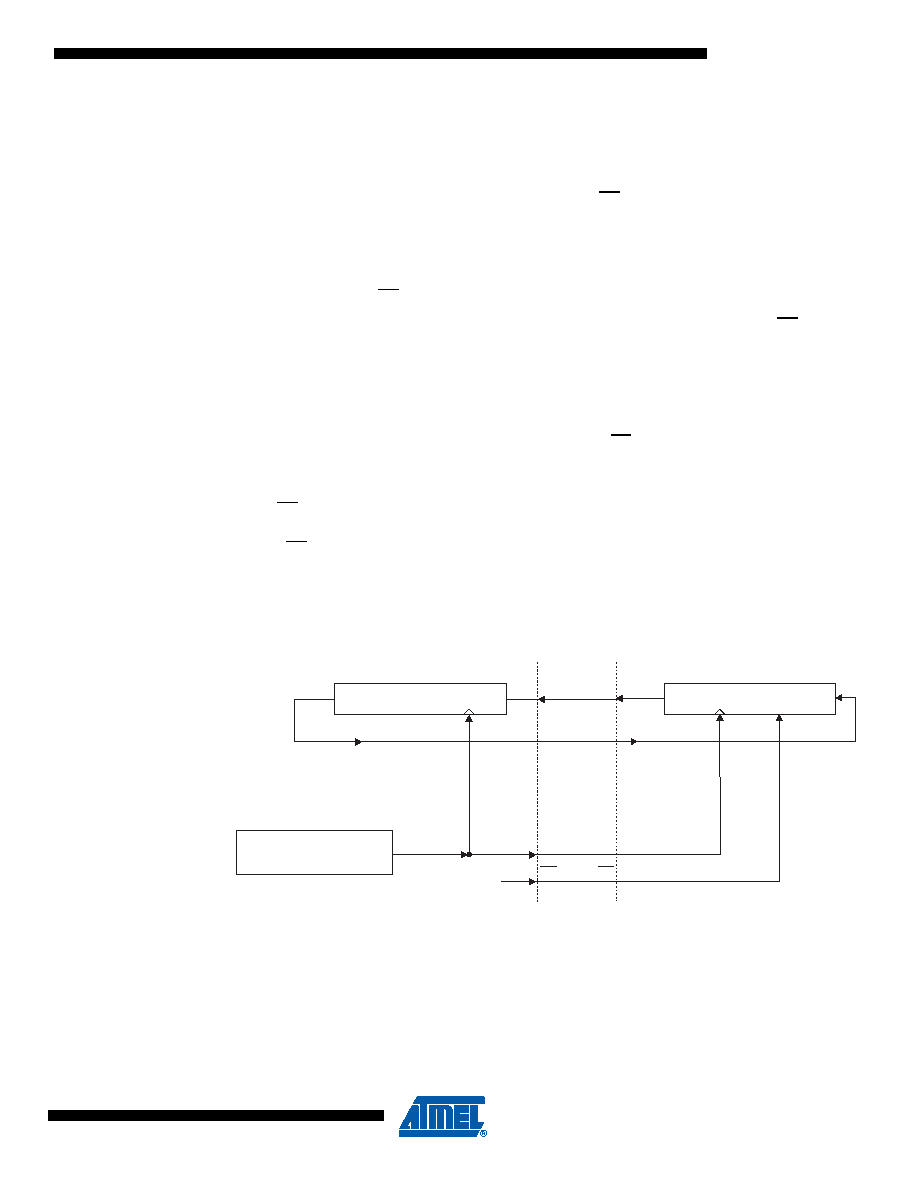
The interconnection between Master and Slave CPUs with SPI is shown in Figure 14-2. The sys-
tem consists of two shift Registers, and a Master clock generator. The SPI Master initiates the
communication cycle when pulling low the Slave Select SS pin of the desired Slave. Master and
Slave prepare the data to be sent in their respective shift Registers, and the Master generates
the required clock pulses on the SCK line to interchange data. Data is always shifted from Mas-
ter to Slave on the Master Out – Slave In, MOSI, line, and from Slave to Master on the Master In
– Slave Out, MISO, line. After each data packet, the Master will synchronize the Slave by pulling
high the Slave Select, SS, line.
When configured as a Master, the SPI interface has no automatic control of the SS line. This
must be handled by user software before communication can start. When this is done, writing a
byte to the SPI Data Register starts the SPI clock generator, and the hardware shifts the eight
bits into the Slave. After shifting one byte, the SPI clock generator stops, setting the end of
Transmission Flag (SPIF). If the SPI Interrupt Enable bit (SPIE) in the SPCR Register is set, an
interrupt is requested. The Master may continue to shift the next byte by writing it into SPDR, or
signal the end of packet by pulling high the Slave Select, SS line. The last incoming byte will be
kept in the Buffer Register for later use.
When configured as a Slave, the SPI interface will remain sleeping with MISO tri-stated as long
as the SS pin is driven high. In this state, software may update the contents of the SPI Data
Register, SPDR, but the data will not be shifted out by incoming clock pulses on the SCK pin
until the SS pin is driven low. As one byte has been completely shifted, the end of Transmission
Flag, SPIF is set. If the SPI Interrupt Enable bit, SPIE, in the SPCR Register is set, an interrupt
is requested. The Slave may continue to place new data to be sent into SPDR before reading
the incoming data. The last incoming byte will be kept in the Buffer Register for later use.
Figure 14-2. SPI Master-slave Interconnection
The system is single buffered in the transmit direction and double buffered in the receive direc-
tion. This means that bytes to be transmitted cannot be written to the SPI Data Register before
the entire shift cycle is completed. When receiving data, however, a received character must be
read from the SPI Data Register before the next character has been completely shifted in. Oth-
erwise, the first byte is lost.
In SPI Slave mode, the control logic will sample the incoming signal of the SCK pin. To ensure
correct sampling of the clock signal, the frequency of the SPI clock should never exceed f
osc/4.
SHIFT
ENABLE
8 BIT SHIFT REGISTER
SPI
CLOCKGENERATOR
MASTER
MSB
MISOMISO
MOSI
SCK
SS
SCK
MOSI
LSB
SLAVE
MSBLSB
8 BIT SHIFT REGISTER
发布紧急采购,3分钟左右您将得到回复。
相关PDF资料
PIC16F87T-E/ML
IC MCU FLASH 4KX14 EEPROM 28QFN
PIC16F87-E/ML
IC MCU FLASH 4KX14 EEPROM 28QFN
PIC18LF4320-I/ML
IC MCU FLASH 4KX16 EEPROM 44QFN
PIC16F77T-I/PTG
IC MCU FLASH 8KX14 W/AD 44TQFP
PIC16LF1933-I/SO
IC PIC MCU FLASH 4K 28-SOIC
PIC16C54C-20I/SO
IC MCU OTP 512X12 18SOIC
PIC16LF726-I/SO
IC PIC MCU FLASH 8K 1.8V 28-SOIC
PIC12CE673-10/P
IC MCU OTP 1KX14 A/D&EE 8DIP
相关代理商/技术参数
PIC16F87T-I/SO
功能描述:8位微控制器 -MCU 7KB 368 RAM 16 I/O RoHS:否 制造商:Silicon Labs 核心:8051 处理器系列:C8051F39x 数据总线宽度:8 bit 最大时钟频率:50 MHz 程序存储器大小:16 KB 数据 RAM 大小:1 KB 片上 ADC:Yes 工作电源电压:1.8 V to 3.6 V 工作温度范围:- 40 C to + 105 C 封装 / 箱体:QFN-20 安装风格:SMD/SMT
PIC16F87T-I/SS
功能描述:8位微控制器 -MCU 7KB 368 RAM 16 I/O RoHS:否 制造商:Silicon Labs 核心:8051 处理器系列:C8051F39x 数据总线宽度:8 bit 最大时钟频率:50 MHz 程序存储器大小:16 KB 数据 RAM 大小:1 KB 片上 ADC:Yes 工作电源电压:1.8 V to 3.6 V 工作温度范围:- 40 C to + 105 C 封装 / 箱体:QFN-20 安装风格:SMD/SMT
PIC16F882-E/ML
功能描述:8位微控制器 -MCU 3.5KB Enh FLSH 128 RAM RoHS:否 制造商:Silicon Labs 核心:8051 处理器系列:C8051F39x 数据总线宽度:8 bit 最大时钟频率:50 MHz 程序存储器大小:16 KB 数据 RAM 大小:1 KB 片上 ADC:Yes 工作电源电压:1.8 V to 3.6 V 工作温度范围:- 40 C to + 105 C 封装 / 箱体:QFN-20 安装风格:SMD/SMT
PIC16F882-E/SO
功能描述:8位微控制器 -MCU 3.5KB Enh FLSH 128 RAM RoHS:否 制造商:Silicon Labs 核心:8051 处理器系列:C8051F39x 数据总线宽度:8 bit 最大时钟频率:50 MHz 程序存储器大小:16 KB 数据 RAM 大小:1 KB 片上 ADC:Yes 工作电源电压:1.8 V to 3.6 V 工作温度范围:- 40 C to + 105 C 封装 / 箱体:QFN-20 安装风格:SMD/SMT
PIC16F882-E/SP
功能描述:8位微控制器 -MCU 3.5KB Enh FLSH 128 RAM RoHS:否 制造商:Silicon Labs 核心:8051 处理器系列:C8051F39x 数据总线宽度:8 bit 最大时钟频率:50 MHz 程序存储器大小:16 KB 数据 RAM 大小:1 KB 片上 ADC:Yes 工作电源电压:1.8 V to 3.6 V 工作温度范围:- 40 C to + 105 C 封装 / 箱体:QFN-20 安装风格:SMD/SMT
PIC16F882-E/SS
功能描述:8位微控制器 -MCU 3.5KB Enh FLSH 128 RAM RoHS:否 制造商:Silicon Labs 核心:8051 处理器系列:C8051F39x 数据总线宽度:8 bit 最大时钟频率:50 MHz 程序存储器大小:16 KB 数据 RAM 大小:1 KB 片上 ADC:Yes 工作电源电压:1.8 V to 3.6 V 工作温度范围:- 40 C to + 105 C 封装 / 箱体:QFN-20 安装风格:SMD/SMT
PIC16F882-I/ML
功能描述:8位微控制器 -MCU 3.5KB Enh FLSH 128 RAM RoHS:否 制造商:Silicon Labs 核心:8051 处理器系列:C8051F39x 数据总线宽度:8 bit 最大时钟频率:50 MHz 程序存储器大小:16 KB 数据 RAM 大小:1 KB 片上 ADC:Yes 工作电源电压:1.8 V to 3.6 V 工作温度范围:- 40 C to + 105 C 封装 / 箱体:QFN-20 安装风格:SMD/SMT
PIC16F882-I/ML
制造商:Microchip Technology Inc 功能描述:IC 8BIT MCU PIC16F 20MHz QFN-28 制造商:Microchip Technology Inc 功能描述:IC, 8BIT MCU, PIC16F, 20MHz, QFN-28